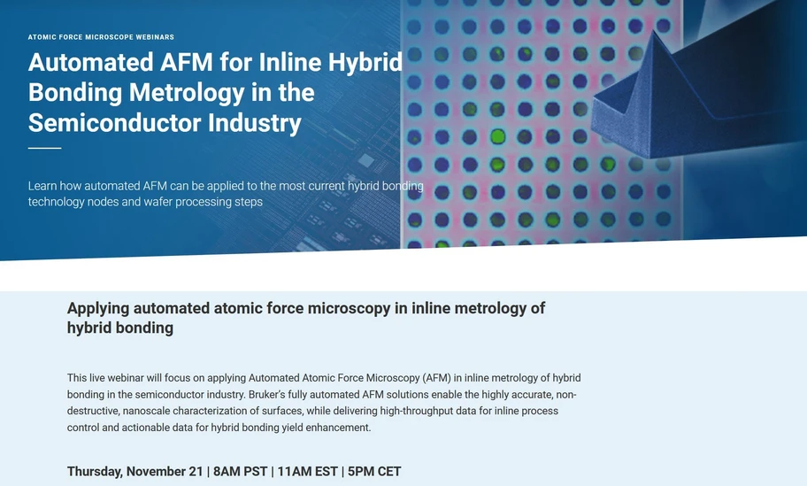
Automated AFM for Inline Hybrid Bonding Metrology in the Semiconductor Industry
This live webinar will focus on applying Automated Atomic Force Microscopy (AFM) in inline metrology of hybrid bonding in the semiconductor industry. Bruker’s fully automated AFM solutions enable the highly accurate, non-destructive, nanoscale characterization of surfaces, while delivering high-throughput data for inline process control and actionable data for hybrid bonding yield enhancement.
In this webinar, we will illustrate how Automated AFM can be applied in the most current hybrid bonding technology nodes and wafer processing steps, and its suitability for labs and fabs working on new bonding device design. The following topics will be discussed:
- Key Automated AFM features for process control in high volume manufacturing of bonded wafers
- High resolution imaging and analysis for critical bond pad metrology
- Large-area scanning of areas of up to 100s of mm2 for large scan topography in wafer-to-wafer bonding
- Automated bevel edge metrology for hybrid bonding
- Patterned and bare/blanket wafer defect review
Don’t miss the opportunity to speak to our experts in the Q&A session!
Presenter: Sean Hand (Senior Staff Applications Scientist, Bruker)
Sean Hand is a Senior Staff Applications Scientist with Bruker's Automated AFM group focused on the application of AFM to semiconductor manufacturing. Sean has an M.S. in physics from the University of Vermont where he focused on Atomic Force Microscopy of lipid bilayers for transdermal drug delivery. Sean has over 25 years of experience in AFM for semiconductor manufacturing and has co-authored over 20 papers and owns several patents related to Automated AFM in semiconductor manufacturing.
Presenter: Ingo Schmitz, Ph.D. (Technical Marketing Engineer, Bruker)
Ingo Schmitz received his Ph.D. in Chemistry from the University of Technology, Vienna Austria in 1996. His Ph.D. work focused on the development of SPM-based in-situ characterization of corrosion processes of glass and metal surfaces. Since 1997, Ingo Schmitz works at Bruker (formerly Digital Instruments & Veeco Instruments) in both Santa Barbara, USA. At Bruker, he held positions as an R&D engineer and application development scientist and contributed in the development of SPM methods including automated surface characterization of polysilicon. Currently, he is working in the technical marketing of automated AFM systems.