Nanoscale AFM-IR Spectroscopy and Imaging for Failure Analysis of Electronic Devices
Due to the systematic shrinking of the size of devices in the semiconductor industry, characterizing nanoscale surface contaminations in interconnects and circuitries has become a pivotal issue in test and failure analysis. Continuous development in process technology/engineering has led to the fabrication of semiconductor devices with sub-µm feature resolution, which in turn demands high-resolution analytical tools for proper characterization.
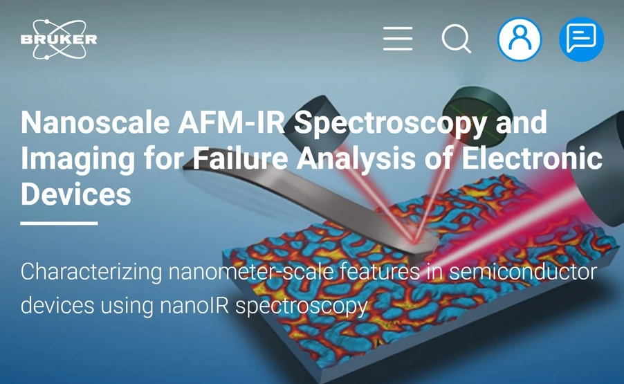
Nanoscale AFM-IR spectroscopy is a non-destructive chemical analysis method that takes advantage of the nanoscale capabilities of AFM and outputs easy-to-understand, FTIR-like spectra. As described by the presenters, the advantages of nanoscale AFM-IR can be leveraged in the semiconductor industry in many ways, like for chemical characterization of organic contaminants, nano-patterned metal/low-k dielectrics, and directed self-assembly of block copolymers.
- watch part 1: Two Complementary Nanoscale IR Techniques: Photothermal AFM-IR and s-SNOM
- watch part 2: Online Demo of the nanoIR3 System - Photothermal AFM-IR
- watch part 3: Chemical Characterization of Heterogenous Polymeric Materials on the Nanoscale Using Photothermal AFM-IR
- watch part 5: 2D Material Characterization Using Photothermal AFM-IR and s-SNOM