Exploring Multi-Field Layer Thickness Capabilities with Micro-XRF in Scanning Electron Microscope
From industrial coatings to ancient fossils, layer thickness analysis using micro-XRF is a powerful technique applied across diverse fields. Bruker micro-XRF for SEM (XTrace 2), combined with XMethod software, enables precise, non-destructive quantification of composition and thickness in complex multilayer structures.
In this webinar, we will introduce the physical principles behind micro-XRF-based layer thickness analysis and demonstrate the layer thickness calculation procedures. You will also see practical workflows using XTrace 2 in object, line, and mapping modes.
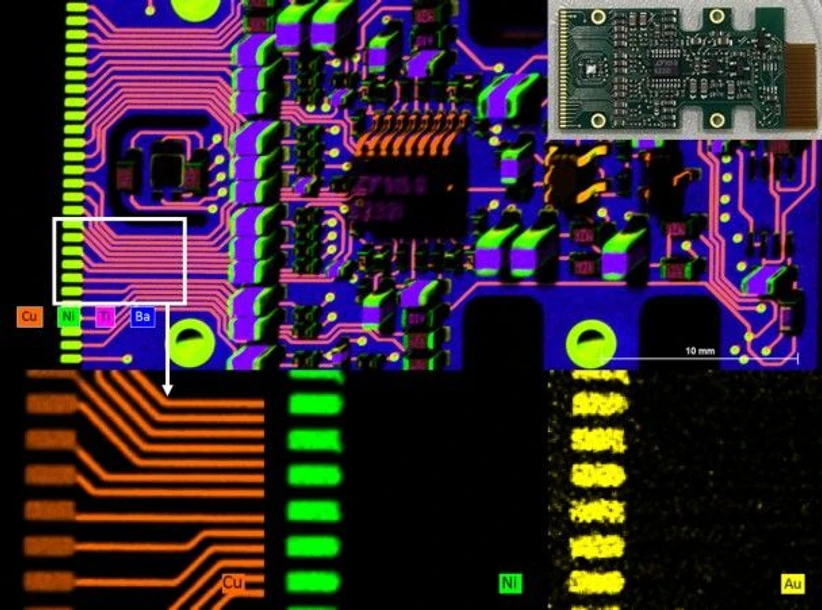 Bruker: Elemental distribution of a printed circuit board (above) and the corresponding elemental distribution of its layer structure build on Cu, Ni and Au (bottom).
We will discuss real-world examples from multiple application fields:
- Multilayer structures in printed circuit boards
- Thin silver layers in photographic samples
- Fossilized trilobite exoskeletons
- Palladium coatings on nickel
- Coatings on silicon wafers
- Standard reference samples with known thicknesses
We will also compare the traditional destructive SEM- and EDS-based methods with the non-destructive micro-XRF method in SEM, highlighting advantages in accuracy, efficiency, and sample preservation.
Who should attend?
- Scientists and researchers from all analytical fields interested in coating thickness calculation in SEM;
- Micro-XRF users;
- Experienced professionals managing electron microscopy labs.
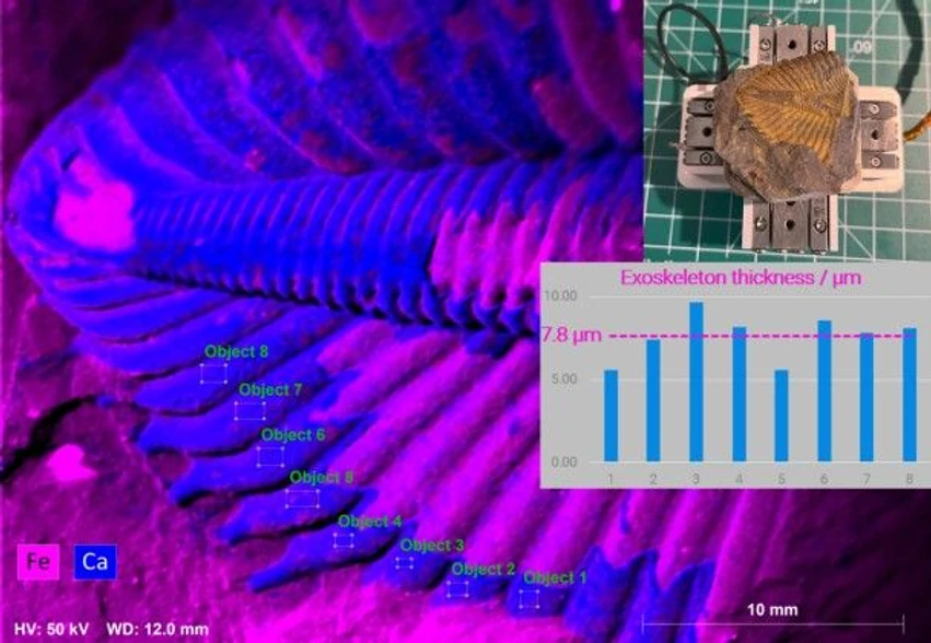 Bruker: Non-destructive thickness evaluation of Trilobite exoskeleton gathered with XTRACE 2 Micro-XRF in SEM. Petrographically, well-kept calcite exoskeleton has ~ 10 µm in thickness.
Presenter: Stephan Boehm (Product Manager - micro-XRF on SEM and WDS, Bruker Electron Microscope Analyzers)
Presenter: Dr. Yang Yang (Application Scientist - micro-XRF on SEM and EDS, Bruker Electron Microscope Analyzers)