Catch Up with eWARP: Unmatched EBSD Performance
Electron Backscatter Diffraction (EBSD) has long been a key technique for microstructural analysis in Scanning Electron Microscopy (SEM), widely adopted across both academic research and industrial applications. From mapping grain orientations in high performance alloys to probing deformation mechanisms in geological samples, EBSD continues to unlock critical insights into material properties.
Our groundbreaking EBSD detector eWARP, which uses Direct Electron Detection (DED) technology, has been changing the EBSD landscape since its launch earlier this year. If you are not yet up to speed with eWARP now is the time to catch up!
This webinar will show you how eWARP, powered by a custom hybrid pixel sensor designed for EBSD applications, redefines EBSD performance by dramatically increasing signal efficiency and acquisition speed.
Curious about how eWARP can enhance your research? We will explore the use of eWARP in a range of applications, from materials science to nanotechnology, to show you what is now possible with the latest EBSD technology.
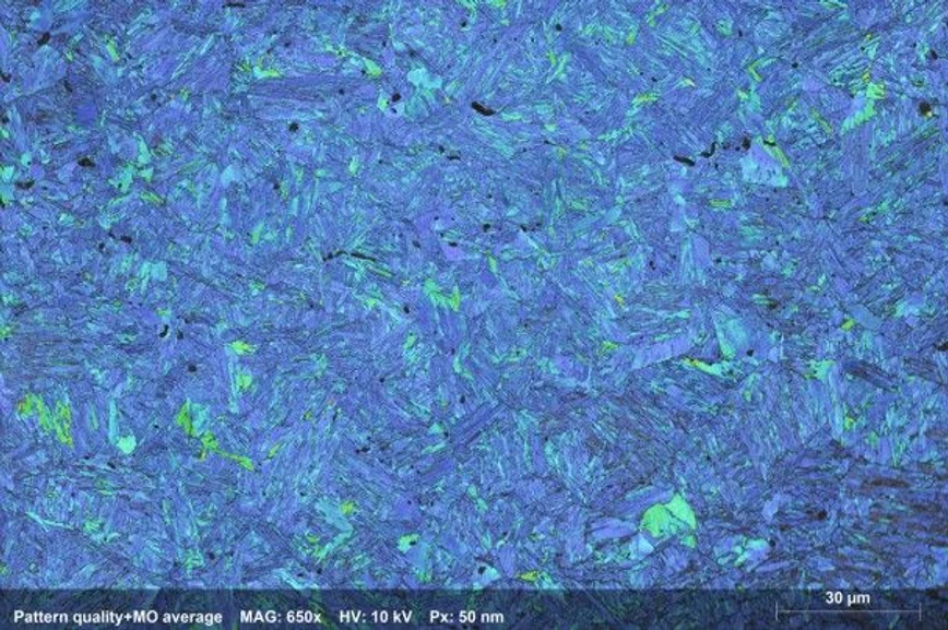 Bruker: Figure 1: Grain Average Misorientation map (false color) of bainitic steel, identifying regions with higher plastic deformation and dislocation density in green and yellow (>6° misorientation).
What to Expect
- Materials Science: See how eWARP enables ultra-fast phase and orientation mapping in complex metallic microstructures, revealing fine precipitates and phase transformation products at unprecedented clarity.
- Battery Research: Discover how high-resolution EBSD measurements quantitatively characterize boundary, grain and texture distributions in battery collector materials.
- Geoscience Applications: EBSD combined EDS phase identification helps you deciphering mineral deformation histories and crystallographic fabrics.
- Nanotechnology: Learn how direct detection pixelated sensor enhances TKD analysis of nanostructured thin films.
- Live Demo: Witness eWARP in action with a real-time EBSD acquisition showcasing its speed and precision.
Whether you're advancing your research or exploring new analytical capabilities, this webinar provides a timely opportunity to learn how next-generation EBSD technology can support and elevate your research.
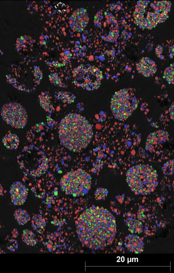 Bruker: Figure 2: Grain Size Distribution map (random coloring) of NMC cathode material used in Lithium-ion battery. In this measurement, 8500 grains were measured with eWARP in only 9 minutes (:measurement speed of 10 000 fps). The average grain size is less than 500 nm. The measurement was done at low accelerating voltage (10 kV) and probe current (13 nA) to reach the required fine step size of 20 nm
Presenter: Dr. Laurie Palasse (Global Application Manager, Bruker Electron Microscope Analyzers)
Presenter: Dr. Meriem Ben Haj Slama (Application Scientist EBSD, Bruker Electron Microscope Analyzers)