QUANTAX WDS: Advancing Microanalysis Beyond the Limits of SEM EDS
Energy Dispersive Spectrometry (EDS) and Wavelength Dispersive Spectrometry (WDS) are complementary techniques for X-ray microanalysis in Scanning Electron Microscopy (SEM). While EDS offers rapid elemental identification, its limitations in spectral resolution and detection sensitivity, particularly for light and trace elements, necessitate a more advanced approach.
QUANTAX WDS addresses these challenges by delivering significantly enhanced spectral resolution (10 to 20 times greater than EDS), lower detection limits (typically 10 times better), and superior performance in light element analysis (up to 50 times higher sensitivity for Boron and Beryllium).
QUANTAX WDS is optimized to provide high spectral resolution for low X-ray energies, enabling high spatialresolution measurement using low accelerating voltages. Consequently, it effectively resolves peak overlaps, confirms elemental presence or absence without reliying on software-based deconvolution, and quantifies elements that EDS may miss. These capabilities extend the analytical reach of elemental identification in SEM, offering reliable detection of trace elements and improved quantification accuracy.
In this webinar, we demonstrate these unique capabilities through diverse application examples from many sectors, automotive, geosciences, steel production, materials research, and semiconductor technology, proving the practical impact of QUANTAX WDS for both industrial and academic research.
This webinar highlights the transformative potential of WDS in modern microanalysis workflows, emphasizing its effectiveness to address the spectral resolution and sensitivity limitations inherent to EDS.
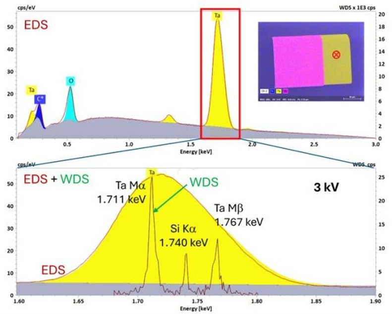 Bruker: Point spectra and map (insert top right) of a semiconductor microsensor sample. EDS only detects Tantalum (and surface-adhering elements C and O). But QUANTAX WDS sees more: it also detects Si, derived from the substrate below the ~30 nm thick Ta layer.
Who should attend
- Researchers and lab managers from industry and academia interested in elemental analysis.
Presenter: Dr. Michael Abratis (Sr. Application Scientist, Bruker Electron Microscope Analyzers)
Presenter: Stephan Boehm (Product Manager - micro-XRF on SEM and WDS, Bruker Electron Microscope Analyzers)